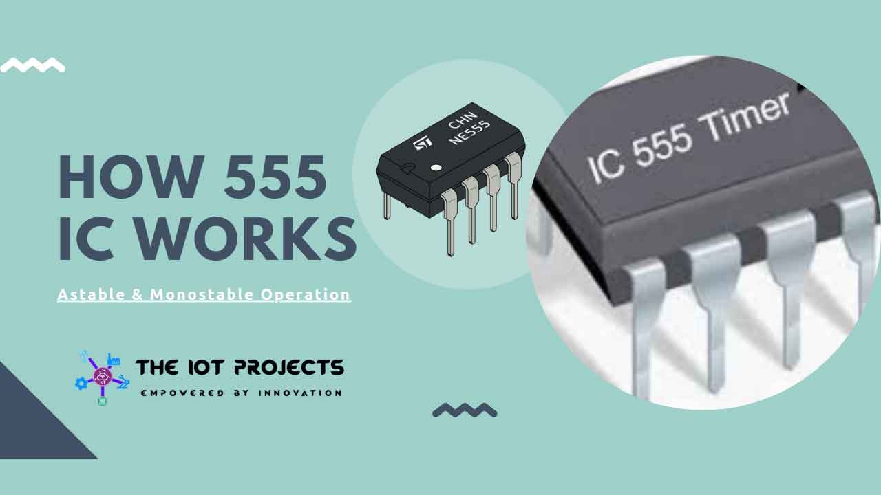
Today in this session we will learn How 555 Timer IC works in Astable operation and Monostable Operation. Actually, 555 Timer IC is an integrated circuit (chip) used in various timer, delay, pulse output, and vibration applications. It was first commercialized by Signetics in 1972.
Introduction to 555 IC
The 555 timer IC is an incredibly useful accurate timer that can be used either as a timer or as a vibrator. In timer mode, it works as monostable mode. Basically, 555 only acts as a “one-shot” timer. When a trigger voltage is applied to its trigger lead, the output of the chip goes from low to high for the period set by the external RC circuit.
In oscillator mode, it acts as an astable mode. The 555 also acts as a Rectangular wave generator whose output waveform (short duration, high duration, frequency, etc.) can be adjusted through two external RC charge/discharge circuits.
For example, with the help of a 555 timer, it is possible to create digital clock waveform generators, LED and light flasher circuits, tone-generator circuits (sirens, metronomes, etc.). likewise, a one-shot timer circuit, bounce-free switches, triangular waveform generators, frequency dividers, etc. can be made using 555 Timer IC.
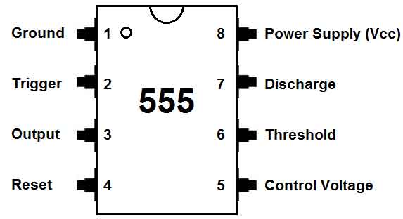
Pinouts
How 555 IC works in Astable Operation?
Below is a block diagram of what is inside the block 555 timer IC. That represents an amazing 555 IC configuration.
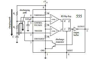
The 555 Its name comes from the three 5-kW resistors as shown in the block diagram. These resistors act as a three-phase voltage separator between the supply voltage (VCC) and the ground. The top of the lower – kW resistor (+ input to comparator 2) is set to 1⁄⁄3 VCC, while the upper mid-kilowatt resistor (input to comparator 1) is set to 2⁄⁄3VCC. Two comparators have outputs of either High or low voltages based on analog voltages compared to their inputs.
If one of the comparator’s positive input is more than its negative input, its output logic level goes higher. If the positive input voltage is lower than the negative input voltage, the output logic level decreases. The outputs of the comparators are sent to the inputs of the SR (set/reset) flip-flop. The flip-flops look at the R and S inputs and produce either high or low based on the voltage state at the input.
How 555 Timer IC works in Monostable Operation?
In monostable mode, there is only one steady state. This means that an externally applied signal is required for the output to switch states.
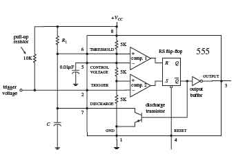
In the monostable configuration, initially (before the trigger pulse is applied) the output of the 555 output is low. The discharges transistor is open, picking up the pin 7 to the ground and keeping the C discharge. Also, pin 2 is usually held up by a 10-k pull-up resistor. Now, when a negative trigger pulse (less than 1/3 VCC) is applied to pin 2, comparator 2 is forced higher, which sets the flip-flop Q‾ to lower. Making the output higher (due to the inverting buffer), while turning off the discharge transistor. This allows C to charge R1 via 0V to VCC.
As far as, across the capacitors, the voltage reaches 2⁄⁄3 VCC, the output of comparator 1 is high, resets the flip flop, and lowers the output, opening the discharge transistor, allows the capacitor to discharge quickly up to 0V. The output will be held in this steady-state. (Low) until another trigger is applied.
The 555 ICs are available in both Polar and CMOS types. Bipolar 555 ICs and CMOS 555s are two types 555 also differ in maximum output current, minimum supply voltage/current, minimum triggering current, and maximum switching speed. With the exception of the maximum output current, the CMOS 555 surpasses the bipolar 555 in all respects. A CMOS 555Timer IC can be distinguished from bipolar 555 IC where part number contains C in the middle (e.g. ICL7555, TLC555, LMC555, etc.).
(Note: that there are hybrid versions of the 555 that incorporate the best features of both bipolar and CMOS technologies.)
Conclusion
Today, you have learned about 555 Timer IC operation modes. Hope you liked this post and don’t forget to share this post with your friends. If you want to know through practical examples. Please let me know in the comment section below.
Recommended Readings:
- BME680 Environment Monitoring System using ESP8266
- Connect RFID to PHP & MySQL Database with NodeMcu ESP8266
- ESP8266 based Coronavirus Tracker for your country
- Password Security Lock System Using Arduino & Keypad
- Electronic Voting Machine Using Arduino & LCD Display
- Internet Clock Using NodeMCU ESP8266 and 16×2 LCD without RTC Module
- IoT Based LED Control using Google Firebase & ESP8266
- Capacitive Soil Moisture Sensor with OLED Display & Arduino
- Secure HTTPS Requests to URL Using NodeMCU ESP8266
- Simple Weather station using Arduino & BME280 Barometric Pressure Sensor
- ESP8266 Plot Sensor readings to Webserver in Real-Time Chart
- IoT Based Voice Controlled Home Automation Using NodeMCU & Android
- RFID Based Attendance System Using NodeMCU with PHP Web App
- NodeMCU ESP8266 Monitoring DHT11/DHT22 Temperature and Humidity with Local Web Server
- Contactless Smart Doorbell Using ESP8266 & Blynk
- ESP8266 Data Logger to Upload Data on Webserver