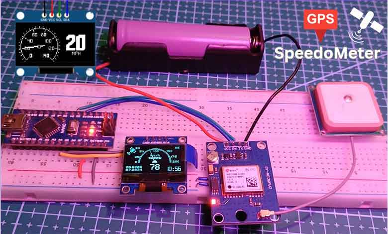
Arduino Speedometer with Neo 6M GPS Module & OLED Display
GPS Speedometer on OLED Display using Arduino
Overview: Arduino GPS Speedometer
This article provides a step-by-step guide on creating a DIY Arduino-based Analog Gauge speedometer using a Neo 6M GPS module. This project aims to measure the speed of a moving object and display it in real time on a 0.96-inch I2C OLED display. The speedometer will showcase the speed in both classic analog gauge style and digital digits. The displayed speed will be measured in miles per hour (MPH).
GPS speedometers are more accurate than traditional speedometers because they can continually track the vehicle’s location and calculate its speed. Traditional speedometers rely on a mechanical cable or sensor to measure the speed of the wheels, which can be affected by factors such as tire wear and road conditions. GPS speedometers, on the other hand, use the Global Positioning System (GPS) to track the vehicle’s location and calculate its speed. GPS is a satellite-based navigation system that provides accurate location information.
You can also check our previous articles on How to Interface NEO 6M GPS V2 Module with Arduino.
Components Required
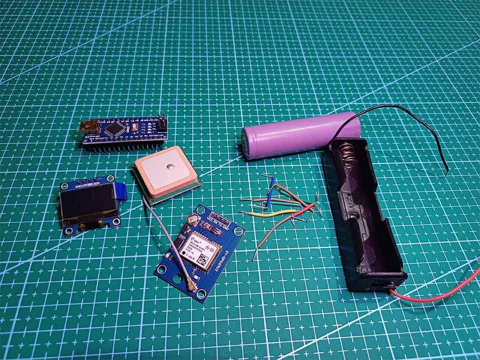
Followings are the list of the components that are required for making an “Arduino Speedometer with Neo 6M GPS Module & OLED Display“. You can easily purchase them from the link provided:
| S.N | COMPONENTS NAME | QUANTITY | PURCHASE LINKS |
|---|---|---|---|
| 1 | Arduino Nano | 1 | Amazon | AliExpress |
| 2 | Neo 6M GPS module | 1 | Amazon | AliExpress |
| 3 | SSD1306 0.96″ OLED display | 1 | Amazon | AliExpress |
| 4 | 18650 Battery Holder | 1 | Amazon | AliExpress |
| 5 | 3.7V 18650 Li-Ion Battery | 1 | Amazon | AliExpress |
| 6 | TP4056 Module | 1 | Amazon | AliExpress |
| 7 | Jumper wires | 10 | Amazon | AliExpress |
| 8 | Breadboard | 1 | Amazon | AliExpress |
*Please Note: These are affiliate links. I may make a commission if you buy the components through these links. I would appreciate your support in this way!
NEO 6M GPS Module
For the Speedometer project will be using the NEO-6M GPS V2 module. The NEO-6M is a popular GPS receiver that has a built-in ceramic antenna, it offers useful satellite search capabilities. With the ability to track up to 22 satellites, it provides accurate location coordinates of your position in the world.
The onboard signal LED indicator will help to monitor the GPS network status. It has a small battery for data backup. With the help of this small battery, GPS module can save data on it’s memory when the main power is shut down.
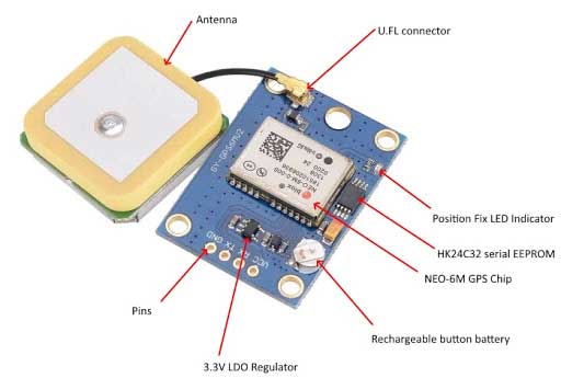
The NEO-6M GPS module uses the powerful NEO-6M GPS chip from u-blox. This chip allows us to track up to 22 satellites on 50 channels. It has a very special sensitivity level which is -161 dBm, meaning it can receive even weak signals effectively.
Specifications of NEO6M GPS Module
- GPS Chip: u-blox NEO-6M
- Satellite Tracking: Up to 22 satellites
- Channels: 50 channels for positioning
- Sensitivity: -161 dBm
- Positioning Engine: u-blox 6
- TTFF: Under 1 second
- Baud Rate: Supports 4800-230400 bps (default: 9600 bps)
- Antenna: Built-in ceramic antenna
- Data Backup: Data backup battery
- Compatibility: Arduino, Raspberry Pi, and other microcontrollers
- Operating Voltage: 3.3V-5V
- Power Consumption: Low power consumption
- Communication: Serial communication (UART)
- Output: NMEA protocol
- Applications: Navigation, tracking, robotics, geocaching, and more.
Pinout of NEO6M GPS Module
Pinout for the NEO-6M GPS Module:
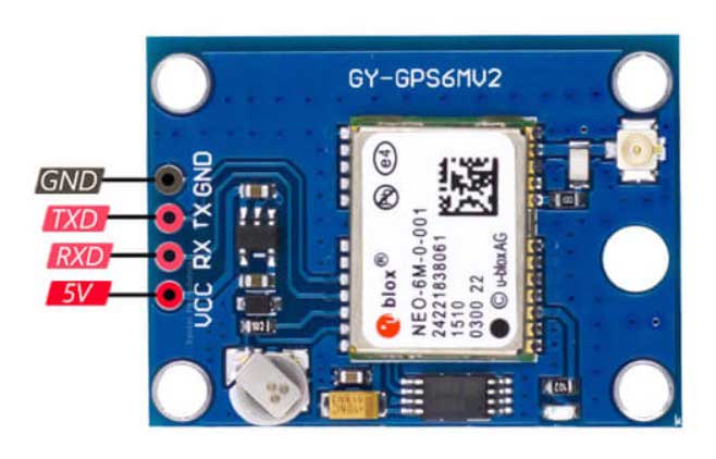
- VCC: Input voltage pin
- RX: Receive pin for UART communication
- TX: Transmit pin for UART communication
- GND: Ground pin
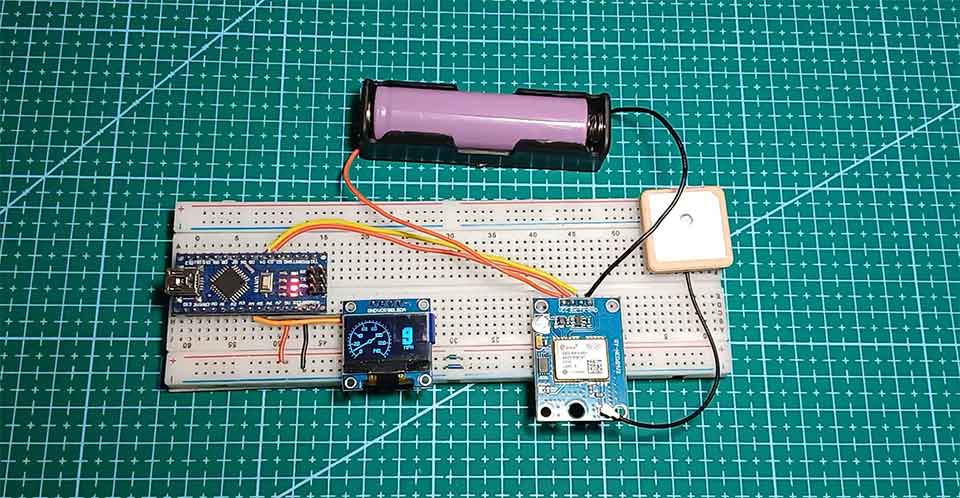
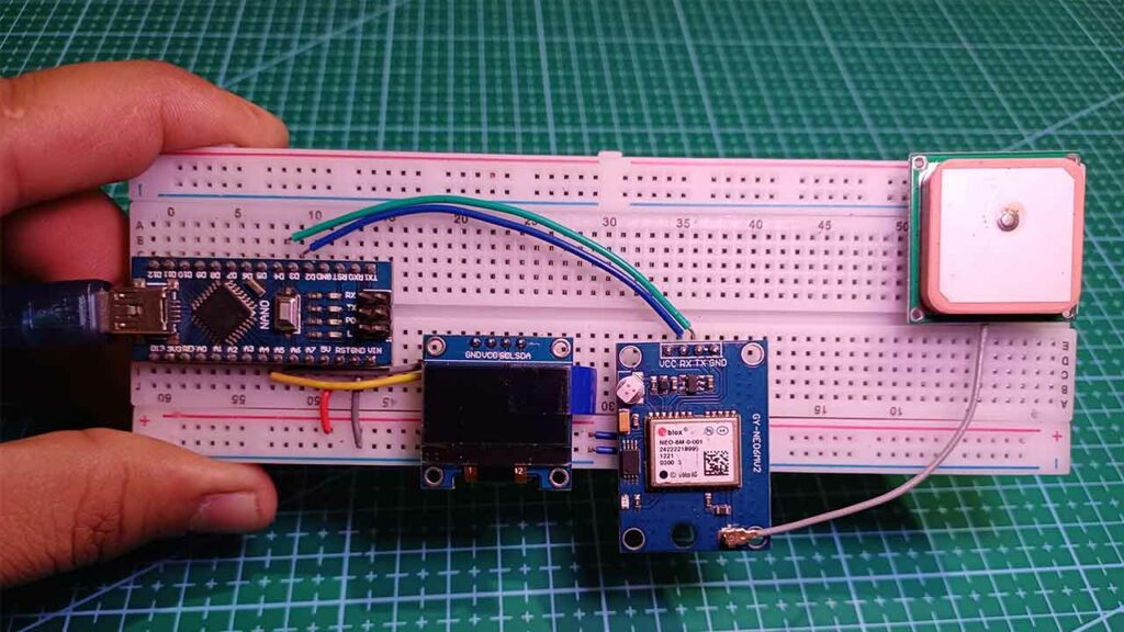
Arduino GPS Speedometer Circuit Diagram
Now let us see the circuit diagram of the Arduino Speedometer with Neo 6M GPS Module & OLED Display. The connection diagram is simple and easy to assemble as shown in the image below.
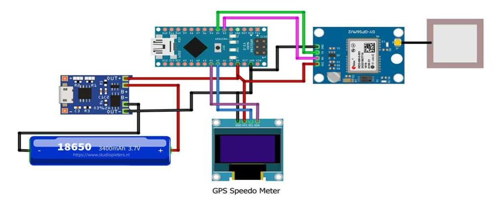
- 1. Connect the VCC pin of the GPS module to the 3.3V pin of the Arduino.
- 2. Connect the GND pin of the GPS module to the GND pin of the Arduino.
- 3. Connect the RX pin of the GPS module to digital pin 3 on the Arduino.
- 4. Connect the TX pin of the GPS module to digital pin 4 on the Arduino.
- 5. Connect the VCC and GND pins of the I2C OLED display to the Arduino’s 5V and GND pins, and connect the SDA and SCL pins to the Arduino’s A4 and A5 pins, respectively.
I have used TP4056 charging module for charging 18650 battery. The whole system is powered with a single 3.7V Li-ion battery. as shown in the above circuit diagram.
NextPCB for PCB Manufacturing Services
In electronics projects, the quality of printed circuit boards (PCBs) plays an important role in the performance and reliability of electronic devices. For my recent project, I was fortunate to have the support and assistance of NextPCB, a leading PCB manufacturer renowned for its wonderful services and commitment to customer satisfaction.
NextPCB offers an extensive range of high-quality, reliable PCBs at competitive prices. Their single-layer PCBs start at just $1.9, while multilayer PCBs start at $6.9. You can also enjoy the free PCB Assembly for 5 boards in your first order. This makes NextPCB an ideal choice for both hobbyists and professionals.
If you are looking for a reliable and cost-effective PCB manufacturer, NextPCB is an excellent choice. With their commitment to quality, fast turnaround times, and value-added services, NextPCB is the ideal partner for your PCB manufacturing needs.
Arduino Source code for GPS Speedometer on OLED
To make program your own Arduino based GPS Speedometer you need to install the following required libraries on Arduino IDE.
Download the TinyGPS++ library and add it to the Arduino library folder.
Download the U8glib library and add it to the Arduino library folder.
There are two different variant of Arduino based GPS Speedometer using Neo 6M GPS Module and 0.96 inch OLED Display.
Simple GPS Speedometer with Analog Gauge & Digital Numbers on OLED
Arduino OLED Speedometer Code.
#include "U8glib.h"

// if you are using SPI version of the display (with 7 pins), comment the first line and uncomment the second line
U8GLIB_SSD1306_128X64 u8g(U8G_I2C_OPT_DEV_0 | U8G_I2C_OPT_NO_ACK | U8G_I2C_OPT_FAST); // Fast I2C / TWI
//U8GLIB_SSD1306_128X64 u8g(13, 11, 8, 9, 10); // SPI connection  - SCL = 13, SDA = 11, RES = 10, DC = 9, CS = 8

#include <SoftwareSerial.h>
#define rxPin 4
#define txPin 3
SoftwareSerial neogps(rxPin,txPin);

#include <TinyGPS++.h> //1.0.3
TinyGPSPlus gps;
double lat;
double lng;
int num_sat, speed;
String heading;

const unsigned char bitmap_center_fill [] PROGMEM = {
	0x00, 0x3c, 0x7e, 0x7e, 0x7e, 0x7e, 0x3c, 0x00
};
// 'center_outline', 8x8px
const unsigned char bitmap_center_outline [] PROGMEM = {
	0x00, 0x3c, 0x42, 0x42, 0x42, 0x42, 0x3c, 0x00
};
// 'gauge_bg', 72x64px
const unsigned char bitmap_gauge_bg [] PROGMEM = {
	0x00, 0x00, 0x00, 0x00, 0x00, 0x00, 0x00, 0x00, 0x00, 0x00, 0x00, 0x00, 0x04, 0x08, 0x20, 0x00,
	0x00, 0x00, 0x00, 0x00, 0x00, 0x04, 0x08, 0x20, 0x00, 0x00, 0x00, 0x00, 0x00, 0x01, 0x00, 0x00,
	0x00, 0x80, 0x00, 0x00, 0x00, 0x00, 0x01, 0x03, 0xff, 0xc0, 0x80, 0x00, 0x00, 0x00, 0x00, 0x20,
	0x3c, 0x00, 0x3c, 0x04, 0x00, 0x00, 0x00, 0x00, 0x21, 0xc0, 0x00, 0x03, 0x84, 0x00, 0x00, 0x00,
	0x00, 0x06, 0x00, 0x00, 0x00, 0x60, 0x00, 0x00, 0x00, 0x00, 0x18, 0x40, 0x00, 0x02, 0x18, 0x00,
	0x00, 0x00, 0x04, 0x20, 0x40, 0x00, 0x02, 0x04, 0x20, 0x00, 0x00, 0x04, 0xc0, 0x20, 0x00, 0x04,
	0x03, 0x20, 0x00, 0x00, 0x01, 0x00, 0x20, 0x00, 0x04, 0x00, 0x80, 0x00, 0x00, 0x02, 0x00, 0x00,
	0x00, 0x00, 0x00, 0x40, 0x00, 0x00, 0x84, 0x00, 0xef, 0x00, 0xcf, 0x00, 0x21, 0x00, 0x00, 0x48,
	0x01, 0x09, 0x01, 0x29, 0x00, 0x12, 0x00, 0x00, 0x10, 0x01, 0xc9, 0x00, 0xc9, 0x00, 0x08, 0x00,
	0x00, 0x20, 0x01, 0x29, 0x01, 0x29, 0x00, 0x04, 0x00, 0x00, 0x40, 0x01, 0x29, 0x01, 0x29, 0x00,
	0x02, 0x00, 0x04, 0x40, 0x00, 0xcf, 0x00, 0xcf, 0x00, 0x02, 0x20, 0x02, 0x80, 0x00, 0x00, 0x00,
	0x00, 0x00, 0x01, 0x40, 0x00, 0x80, 0x00, 0x00, 0x00, 0x00, 0x00, 0x01, 0x00, 0x01, 0x20, 0x00,
	0x00, 0x00, 0x00, 0x00, 0x04, 0x80, 0x02, 0x18, 0x00, 0x00, 0x00, 0x00, 0x00, 0x18, 0x40, 0x22,
	0x04, 0x00, 0x00, 0x00, 0x00, 0x00, 0x20, 0x44, 0x14, 0x01, 0x2f, 0x00, 0x00, 0x02, 0xf7, 0x80,
	0x28, 0x04, 0x01, 0x29, 0x00, 0x00, 0x02, 0x94, 0x80, 0x20, 0x04, 0x01, 0xe9, 0x00, 0x00, 0x02,
	0x94, 0x80, 0x20, 0x08, 0x00, 0x29, 0x00, 0x00, 0x02, 0x94, 0x80, 0x10, 0x08, 0x00, 0x29, 0x00,
	0x00, 0x02, 0x94, 0x80, 0x10, 0xc8, 0x00, 0x2f, 0x00, 0x00, 0x02, 0xf7, 0x80, 0x13, 0x08, 0x00,
	0x00, 0x00, 0x00, 0x00, 0x00, 0x00, 0x10, 0x10, 0x00, 0x00, 0x00, 0x00, 0x00, 0x00, 0x00, 0x08,
	0x10, 0x00, 0x00, 0x00, 0x00, 0x00, 0x00, 0x00, 0x08, 0x10, 0x00, 0x00, 0x00, 0x00, 0x00, 0x00,
	0x00, 0x08, 0x10, 0x00, 0x00, 0x00, 0x00, 0x00, 0x00, 0x00, 0x08, 0xd0, 0x00, 0x00, 0x00, 0x00,
	0x00, 0x00, 0x00, 0x0b, 0x10, 0x00, 0x00, 0x00, 0x00, 0x00, 0x00, 0x00, 0x08, 0x10, 0x39, 0xe0,
	0x00, 0x00, 0x00, 0x17, 0x3c, 0x08, 0x10, 0x05, 0x20, 0x00, 0x00, 0x00, 0x10, 0xa4, 0x08, 0x10,
	0x09, 0x20, 0x00, 0x00, 0x00, 0x11, 0x24, 0x08, 0x17, 0x91, 0x20, 0x00, 0x00, 0x00, 0x12, 0x25,
	0xe8, 0xd0, 0x21, 0x20, 0x00, 0x00, 0x00, 0x14, 0x24, 0x0b, 0x10, 0x3d, 0xe0, 0x00, 0x00, 0x00,
	0x17, 0xbc, 0x08, 0x08, 0x00, 0x00, 0x00, 0x00, 0x00, 0x00, 0x00, 0x10, 0x08, 0x00, 0x00, 0x00,
	0x00, 0x00, 0x00, 0x00, 0x10, 0x08, 0x00, 0x00, 0x00, 0x00, 0x00, 0x00, 0x00, 0x10, 0x08, 0x00,
	0x00, 0x00, 0x00, 0x00, 0x00, 0x00, 0x10, 0x64, 0x00, 0x00, 0x00, 0x00, 0x00, 0x00, 0x00, 0x26,
	0x04, 0x00, 0x00, 0x00, 0x00, 0x00, 0x00, 0x00, 0x20, 0x04, 0x00, 0x00, 0x00, 0x00, 0x00, 0x00,
	0x00, 0x20, 0x02, 0x00, 0x1e, 0x00, 0x00, 0x29, 0x78, 0x00, 0x40, 0x02, 0x00, 0x12, 0x00, 0x00,
	0x29, 0x48, 0x00, 0x40, 0x09, 0x00, 0x12, 0x00, 0x00, 0x2f, 0x48, 0x00, 0x90, 0x11, 0x00, 0x12,
	0x00, 0x00, 0x21, 0x48, 0x00, 0x88, 0x00, 0x80, 0x12, 0x00, 0x00, 0x21, 0x48, 0x01, 0x00, 0x00,
	0x40, 0x1e, 0x00, 0x00, 0x21, 0x78, 0x02, 0x00, 0x00, 0x40, 0x40, 0x00, 0x00, 0x00, 0x02, 0x02,
	0x00, 0x00, 0x20, 0x80, 0x00, 0x00, 0x00, 0x01, 0x04, 0x00, 0x01, 0x11, 0x00, 0x00, 0x00, 0x00,
	0x00, 0x88, 0x80, 0x02, 0x0a, 0x00, 0x00, 0x00, 0x00, 0x00, 0x50, 0x40, 0x00, 0x04, 0x00, 0x00,
	0x00, 0x00, 0x00, 0x20, 0x00, 0x00, 0x00, 0x00, 0x00, 0x00, 0x00, 0x00, 0x00, 0x00, 0x00, 0x10,
	0x00, 0x00, 0x00, 0x00, 0x00, 0x08, 0x00, 0x00, 0x20, 0x00, 0x00, 0x00, 0x00, 0x00, 0x04, 0x00
};
// 'mph_label', 16x6px
const unsigned char bitmap_mph_label [] PROGMEM = {
	0x8b, 0xd2, 0xda, 0x52, 0xab, 0xde, 0x8a, 0x12, 0x8a, 0x12, 0x8a, 0x12
};

// 'digit_0', 16x28px
const unsigned char bitmap_digit_0 [] PROGMEM = {
	0x0f, 0xff, 0x1f, 0xff, 0x7f, 0xff, 0xff, 0xff, 0xff, 0xff, 0xff, 0xff, 0xfc, 0x3f, 0xfc, 0x3f,
	0xfc, 0x3f, 0xfc, 0x3f, 0xfc, 0x3f, 0xfc, 0x3f, 0xfc, 0x3f, 0xfc, 0x3f, 0xfc, 0x3f, 0xfc, 0x3f,
	0xfc, 0x3f, 0xfc, 0x3f, 0xfc, 0x3f, 0xfc, 0x3f, 0xfc, 0x3f, 0xfc, 0x3f, 0xfc, 0x3f, 0xff, 0xff,
	0xff, 0xff, 0xff, 0xfe, 0xff, 0xfc, 0xff, 0xf8
};
// 'digit_1', 16x28px
const unsigned char bitmap_digit_1 [] PROGMEM = {
	0x01, 0xf8, 0x03, 0xf8, 0x07, 0xf8, 0x1f, 0xf8, 0x1f, 0xf8, 0x1f, 0xf8, 0x1f, 0xf8, 0x1f, 0xf8,
	0x01, 0xf8, 0x01, 0xf8, 0x01, 0xf8, 0x01, 0xf8, 0x01, 0xf8, 0x01, 0xf8, 0x01, 0xf8, 0x01, 0xf8,
	0x01, 0xf8, 0x01, 0xf8, 0x01, 0xf8, 0x01, 0xf8, 0x01, 0xf8, 0x01, 0xf8, 0x01, 0xf8, 0x01, 0xf8,
	0x01, 0xf8, 0x01, 0xf8, 0x01, 0xf8, 0x01, 0xf8
};
// 'digit_2', 16x28px
const unsigned char bitmap_digit_2 [] PROGMEM = {
	0x0f, 0xfe, 0x1f, 0xff, 0x3f, 0xff, 0x7f, 0xff, 0xff, 0xff, 0xff, 0xff, 0xfc, 0x3f, 0xfc, 0x3f,
	0xfc, 0x3f, 0x00, 0x3f, 0x00, 0x7f, 0x00, 0xff, 0x01, 0xfe, 0x03, 0xfc, 0x0f, 0xf8, 0x1f, 0xf0,
	0x3f, 0xe0, 0x7f, 0xc0, 0xff, 0x00, 0xfe, 0x00, 0xfc, 0x00, 0xfc, 0x00, 0xfc, 0x00, 0xff, 0xff,
	0xff, 0xff, 0xff, 0xff, 0xff, 0xff, 0xff, 0xff
};
// 'digit_3', 16x28px
const unsigned char bitmap_digit_3 [] PROGMEM = {
	0x0f, 0xfe, 0x3f, 0xff, 0x7f, 0xff, 0xff, 0xff, 0xff, 0xff, 0xff, 0xff, 0xf8, 0x3f, 0xf8, 0x3f,
	0xf8, 0x3f, 0x00, 0x3f, 0x00, 0x3f, 0x00, 0xfe, 0x00, 0xfc, 0x00, 0xf8, 0x00, 0xff, 0x00, 0xff,
	0x00, 0xff, 0x00, 0x3f, 0x00, 0x3f, 0xf8, 0x3f, 0xf8, 0x3f, 0xf8, 0x3f, 0xfc, 0x3f, 0xff, 0xff,
	0xff, 0xff, 0xff, 0xfe, 0xff, 0xfc, 0xff, 0xf8
};
// 'digit_4', 16x28px
const unsigned char bitmap_digit_4 [] PROGMEM = {
	0x00, 0x70, 0x00, 0x78, 0x00, 0xfc, 0x00, 0xfe, 0x01, 0xff, 0x03, 0xff, 0x03, 0xff, 0x07, 0xff,
	0x07, 0xff, 0x0f, 0xff, 0x0f, 0xbf, 0x1f, 0xbf, 0x1f, 0x3f, 0x3f, 0x3f, 0x3e, 0x3f, 0x7e, 0x3f,
	0x7c, 0x3f, 0xfc, 0x3f, 0xff, 0xff, 0x7f, 0xff, 0x3f, 0xff, 0x3f, 0xff, 0x1f, 0xff, 0x00, 0x3f,
	0x00, 0x3f, 0x00, 0x3f, 0x00, 0x3f, 0x00, 0x3f
};
// 'digit_5', 16x28px
const unsigned char bitmap_digit_5 [] PROGMEM = {
	0x7f, 0xfe, 0xff, 0xfe, 0xff, 0xfe, 0xff, 0xfe, 0xff, 0xfe, 0xff, 0xfe, 0xfc, 0x00, 0xfc, 0x00,
	0xfc, 0x00, 0xfc, 0x00, 0xfe, 0x00, 0xff, 0xf0, 0xff, 0xf8, 0xff, 0xfe, 0xff, 0xfe, 0xff, 0xff,
	0x00, 0x3f, 0x00, 0x3f, 0x00, 0x3f, 0xfc, 0x3f, 0xfc, 0x3f, 0xfc, 0x3f, 0xfc, 0x7f, 0xff, 0xff,
	0xff, 0xff, 0x7f, 0xff, 0x3f, 0xff, 0x1f, 0xff
};
// 'digit_6', 16x28px
const unsigned char bitmap_digit_6 [] PROGMEM = {
	0x0f, 0xfe, 0x1f, 0xff, 0x3f, 0xff, 0x7f, 0xff, 0xff, 0xff, 0xff, 0xff, 0xfc, 0x3f, 0xfc, 0x3f,
	0xfc, 0x3f, 0xfc, 0x00, 0xfc, 0x00, 0xff, 0xfe, 0xff, 0xff, 0xff, 0xff, 0xff, 0xff, 0xff, 0xff,
	0xff, 0xff, 0xfc, 0x3f, 0xfc, 0x3f, 0xfc, 0x3f, 0xfc, 0x3f, 0xfc, 0x3f, 0xfc, 0x7f, 0xff, 0xff,
	0xff, 0xfe, 0xff, 0xfc, 0xff, 0xf8, 0xff, 0xf0
};
// 'digit_7', 16x28px
const unsigned char bitmap_digit_7 [] PROGMEM = {
	0xff, 0xf0, 0xff, 0xf8, 0xff, 0xfc, 0xff, 0xfe, 0xff, 0xff, 0xff, 0xff, 0xf8, 0x3e, 0xf8, 0x7e,
	0xf8, 0x7e, 0x00, 0xfc, 0x00, 0xfc, 0x00, 0xfc, 0x01, 0xf8, 0x01, 0xf8, 0x01, 0xf8, 0x03, 0xf0,
	0x03, 0xf0, 0x07, 0xf0, 0x07, 0xe0, 0x07, 0xe0, 0x0f, 0xc0, 0x0f, 0xc0, 0x0f, 0xc0, 0x1f, 0x80,
	0x1f, 0x80, 0x3f, 0x80, 0x3f, 0x00, 0x3f, 0x00
};
// 'digit_8', 16x28px
const unsigned char bitmap_digit_8 [] PROGMEM = {
	0x0f, 0xfe, 0x1f, 0xfe, 0x3f, 0xfe, 0x7f, 0xfe, 0xff, 0xfe, 0xff, 0xfe, 0xfc, 0x3e, 0xfc, 0x3e,
	0xfc, 0x3e, 0xfc, 0x3e, 0xfc, 0x3e, 0xfc, 0x3e, 0xff, 0xfc, 0xff, 0xf8, 0x1f, 0xff, 0x7f, 0xff,
	0xff, 0xff, 0xfc, 0x3f, 0xfc, 0x3f, 0xfc, 0x3f, 0xfc, 0x3f, 0xfc, 0x3f, 0xfc, 0x3f, 0xff, 0xff,
	0xff, 0xff, 0xff, 0xfe, 0xff, 0xfc, 0xff, 0xf8
};
// 'digit_9', 16x28px
const unsigned char bitmap_digit_9 [] PROGMEM = {
	0x07, 0xff, 0x1f, 0xff, 0x3f, 0xff, 0x7f, 0xff, 0xff, 0xff, 0xff, 0xff, 0xfc, 0x3f, 0xfc, 0x3f,
	0xfc, 0x3f, 0xfc, 0x3f, 0xfc, 0x3f, 0xff, 0xff, 0xff, 0xff, 0xff, 0xff, 0xff, 0xff, 0xff, 0xff,
	0xff, 0xff, 0x00, 0x3f, 0x00, 0x3f, 0xfc, 0x3f, 0xfc, 0x3f, 0xfc, 0x3f, 0xfc, 0x3f, 0xff, 0xff,
	0xff, 0xff, 0xff, 0xfe, 0xff, 0xfc, 0xff, 0xf8
};

// Array of all bitmaps for convenience. (Total bytes used to store images in PROGMEM = 800)
const int bitmap_allArray_LEN = 10;
const unsigned char* bitmap_allArray[10] = {
	bitmap_digit_0,
	bitmap_digit_1,
	bitmap_digit_2,
	bitmap_digit_3,
	bitmap_digit_4,
	bitmap_digit_5,
	bitmap_digit_6,
	bitmap_digit_7,
	bitmap_digit_8,
	bitmap_digit_9
};

char speed_string[10]; // speed number value converted to c-style string (array of characters)
int speed_string_length; // length of the speed_string
int speed_string_start_pos; // start x position for the big numbers - calculated based on the number of digits

int needle_angle_deg = 45; // angle of the needle in degrees, based on potentiometer value

int needle_start_x; // needle start point, x position
int needle_start_y; // needle start point, y position
int needle_end_x; // needle end point, x position
int needle_end_y; // needle end point, y position
int needle_center_x = 36; // needle center position, x position
int needle_center_y = 36; // needle center position, y position
int needle_radius_big = 30; // lenght of needle
int needle_radius_small = 10; // lenght of "tail" of the needle
int needle_offset_x; // second line offset x
int needle_offset_y; // second line offset y

void setup() {
  Serial.begin(9600);
  neogps.begin(9600);
  u8g.setFont(u8g_font_tpssb); // set u8g font, although this is not used anywhere
  u8g.setColorIndex(1); // set drawing color to white

}

void Read_GPS(){
  //------------------------------------------------------------------
  boolean newData = false;
  for (unsigned long start = millis(); millis() - start < 1000;)
  {
    while (neogps.available())
    {
      if (gps.encode(neogps.read()))
      {
        newData = true;
        break;
      }
    }
  }
  //------------------------------------------------------------------
  //If newData is true
  if(newData == true){
    newData = false;
    Get_GPS();
  }
  else {
    //no data
  }
}

void Get_GPS(){
  num_sat = gps.satellites.value();

  if (gps.location.isValid() == 1) {
    speed = gps.speed.kmph();
    Serial.print("Speed: ");Serial.println(speed);
    lat = gps.location.lat();
    Serial.print("lat: ");Serial.println(lat);
    lng = gps.location.lng();
    Serial.print("lng: ");Serial.println(lng);
    heading = gps.cardinal(gps.course.value());
    Serial.print("heading: ");Serial.println(heading);
  }
}

void loop() {
  Read_GPS();

  //if(speed>140)
  //speed=0;

  itoa (speed, speed_string, 10); // convert speed integer to c-style string speed_string, decimal format
  speed_string_length = strlen(speed_string); // get speed_string length
  speed_string_start_pos = 99 - speed_string_length * 8; // start x position of the big numbers

  needle_angle_deg = map(speed, 0, 140, 45, 270+45); // calculate the angle in degrees based on the speed value, between 45-315

  needle_start_x = needle_radius_big * -sin(radians(needle_angle_deg)) + needle_center_x; // calculate needle start x position
  needle_start_y = needle_radius_big *  cos(radians(needle_angle_deg)) + needle_center_y; // calculate needle start y position

  needle_end_x = needle_radius_small * -sin(radians(needle_angle_deg + 180)) + needle_center_x; // calculate needle end x position
  needle_end_y = needle_radius_small *  cos(radians(needle_angle_deg + 180)) + needle_center_y; // calculate needle end y position

  // calculate offset for the second line for the needle, based on the needle slope
  if ((needle_angle_deg > 45 && needle_angle_deg < 135) || (needle_angle_deg > 225 && needle_angle_deg < 315)) {
    // needle is more horizontal, offset the second line by y
    needle_offset_x = 0;
    needle_offset_y = 1;
  } else {
    // needle is more vertical, offset the second line by x
    needle_offset_x = 1;
    needle_offset_y = 0;
  }

  u8g.firstPage(); // u8g drawing
  do {

     //u8g.drawStr(90, 20, speed_string); // draw speed_string, not needed anymore

     for (int i = 0; i < speed_string_length; i++) { // loop for every speed_string character
       // draw the big digit
       // subtract value 45 from the character value, since the ASCII value of digit "0" is 48
       u8g.drawBitmapP(speed_string_start_pos + 18 * i, 16, 16/8, 28, bitmap_allArray[speed_string[i] - 48]);
     }

     u8g.drawBitmapP(  0,  0, 72/8, 64, bitmap_gauge_bg); // draw gauge background image

     u8g.drawLine(needle_start_x, needle_start_y, needle_end_x, needle_end_y); // draw first line for the needle
     u8g.drawLine(needle_start_x+needle_offset_x, needle_start_y+needle_offset_y, needle_end_x+needle_offset_x, needle_end_y+needle_offset_y); // draw second line for the needle

     u8g.setColorIndex(0); // black color
     u8g.drawBitmapP( 32, 33,  8/8,  8, bitmap_center_fill); // draw needle center cover
     u8g.setColorIndex(1); // white color
     u8g.drawBitmapP( 32, 33,  8/8,  8, bitmap_center_outline); // draw needle center piece

     u8g.drawBitmapP( 93, 46, 16/8,  6, bitmap_mph_label); // draw MPH label


  } while ( u8g.nextPage() );
//--------------------------------
}
GPS Speedometer with Gauge & NTP Clock on OLED
Arduino OLED Speedometer Code – Odometer with Analog Gauge and NTP Clock, Location coordinates, and Number of satellites connected.
//---------------------------------------------------------------------------
#include "U8glib.h"
U8GLIB_SSD1306_128X64 u8g(U8G_I2C_OPT_NONE|U8G_I2C_OPT_DEV_0);
//---------------------------------------------------------------------------
const int timezone_hours = 5;
const int timezone_minutes = 0;
//---------------------------------------------------------------------------
#include <SoftwareSerial.h>
#define rxPin 4
#define txPin 3
SoftwareSerial neogps(rxPin,txPin);

#include <TinyGPS++.h> //1.0.3
TinyGPSPlus gps;
//---------------------------------------------------------------------------
int x_max    = 128;       //OLED display width, in pixels
int y_max    = 62;        //OLED display width, in pixels
int x_center = x_max/2;
int y_center = y_max/2+10;
int arc      = y_max/2;
int angle    = 0;
//---------------------------------------------------------------------------
int needle_pos = 0;
u8g_uint_t xx  = 0;
//---------------------------------------------------------------------------
//satellite logo
#define sat_logo_width 20
#define sat_logo_height 20

const unsigned char sat_logo[] = {
  0x00, 0x01, 0x00, 0x80, 0x07, 0x00, 0xc0, 0x06, 0x00, 0x60, 0x30, 0x00,
  0x60, 0x78, 0x00, 0xc0, 0xfc, 0x00, 0x00, 0xfe, 0x01, 0x00, 0xff, 0x01,
  0x80, 0xff, 0x00, 0xc0, 0x7f, 0x06, 0xc0, 0x3f, 0x06, 0x80, 0x1f, 0x0c,
  0x80, 0x4f, 0x06, 0x19, 0xc6, 0x03, 0x1b, 0x80, 0x01, 0x73, 0x00, 0x00,
  0x66, 0x00, 0x00, 0x0e, 0x00, 0x00, 0x3c, 0x00, 0x00, 0x70, 0x00, 0x00
};
//---------------------------------------------------------------------------

//Program variables
double lat;
double lng;
//int day, month, year;
String hours, minutes;
int second;

int num_sat, speed;
String heading;


/*******************************************************************************************
 * gauge function
 * dispay gauge and other gps data on oled
*******************************************************************************************/
void gauge(uint8_t angle) {
  //fonts: u8g_font_chikita - u8g_font_04b_03br
  // u8g_font_orgv01 - u8g_font_freedoomr10r
  u8g.setFont(u8g_font_chikita);
  //---------------------------------------------------------------------------
  // draw border of the gauge
  u8g.drawCircle(x_center,y_center,arc+6, U8G_DRAW_UPPER_RIGHT);
  u8g.drawCircle(x_center,y_center,arc+4, U8G_DRAW_UPPER_RIGHT);
  u8g.drawCircle(x_center,y_center,arc+6, U8G_DRAW_UPPER_LEFT);
  u8g.drawCircle(x_center,y_center,arc+4, U8G_DRAW_UPPER_LEFT);
  //---------------------------------------------------------------------------
  // show gauge values
  u8g.drawStr(20,  42, "0");
  u8g.drawStr(18,  29, "25");
  u8g.drawStr(28,  14, "50");
  u8g.drawStr(60,  14, "100");
  u8g.drawStr(91,  14, "150");
  u8g.drawStr(101, 29, "175");
  u8g.drawStr(105, 42, "200");
  //---------------------------------------------------------------------------
  // show gauge label
  u8g.setPrintPos(54,25);
  u8g.print("km/h");
  u8g.setPrintPos(50,32);
  u8g.print("SPEED");
  //---------------------------------------------------------------------------
  // draw the needle
  float x1=sin(2*angle*2*3.14/360);
  float y1=cos(2*angle*2*3.14/360);
  u8g.drawLine(x_center, y_center, x_center+arc*x1, y_center-arc*y1);
  u8g.drawDisc(x_center, y_center, 5, U8G_DRAW_UPPER_LEFT);
  u8g.drawDisc(x_center, y_center, 5, U8G_DRAW_UPPER_RIGHT);
  //---------------------------------------------------------------------------
  //TOP LEFT: draw satellite logo and number of satellites
  u8g.drawXBM(0, 0, sat_logo_width, sat_logo_height, sat_logo);
  u8g.setPrintPos(18, 5);
  u8g.print(num_sat, 5);
  //---------------------------------------------------------------------------
  //TOP RIGHT: Display direction
  u8g.setPrintPos(110, 5);
  u8g.print(heading);
  //---------------------------------------------------------------------------
  //Display latitude and longitude
  u8g.setPrintPos(0, 55);
  u8g.print(lat, 4);
  u8g.setPrintPos(0, 62);
  u8g.print(lng, 4);
  //---------------------------------------------------------------------------
  //Display time
  u8g.setFont(u8g_font_freedoomr10r);
  u8g.setPrintPos(90, 65);
  u8g.print(hours);

  if(second%2 == 0)
    {u8g.drawStr(104, 65, ":");}
  else
    {u8g.drawStr(104, 65, " ");}

  u8g.setPrintPos(111, 65);
  u8g.print(minutes);

  //u8g.drawStr(90, 65, "00:00");
  //---------------------------------------------------------------------------
  // Show Speed and align its position
  u8g.setFont(u8g_font_profont22);
  u8g.setPrintPos(54,60);
  if (speed<10){
    u8g.print("0");
  }
  if (speed>99) {
    u8g.setPrintPos(47,60);
  }
  u8g.print(speed);
  //---------------------------------------------------------------------------
}

/*******************************************************************************************
 * gauge function
 * dispay gauge and other gps data on oled
*******************************************************************************************/
int i = 200;
void setup(void) {
  Serial.begin(9600);

  neogps.begin(9600);

  u8g.setFont(u8g_font_chikita);
  u8g.setColorIndex(1);
}

/*******************************************************************************************
 * gauge function
 * dispay gauge and other gps data on oled
*******************************************************************************************/
void loop(void){
  //----------------------------------------------------------
  Read_GPS();
  //----------------------------------------------------------
  needle_pos = map(speed,0,200,0,90); //SET NEEDLE
  // show needle and dial
  xx = needle_pos;
  if (xx<45)
    {xx=xx+135;}
  else
    {xx=xx-45;}
  //----------------------------------------------------------
  //Display Data on Oled
  {
    u8g.firstPage();
    do {
      gauge(xx);
    }
    while( u8g.nextPage() );
  }
  //----------------------------------------------------------
}


void Read_GPS(){
  //------------------------------------------------------------------
  boolean newData = false;
  for (unsigned long start = millis(); millis() - start < 1000;)
  {
    while (neogps.available())
    {
      if (gps.encode(neogps.read()))
      {
        newData = true;
        break;
      }
    }
  }
  //------------------------------------------------------------------
  //If newData is true
  if(newData == true){
    newData = false;
    Get_GPS();
  }
  else {
    //no data
  }
}


void Get_GPS(){
  num_sat = gps.satellites.value();

  if (gps.location.isValid() == 1) {
    speed = gps.speed.kmph();
    //Serial.print("Speed: ");Serial.println(gps_speed);
    lat = gps.location.lat();
    //Serial.print("lat: ");Serial.println(lat);
    lng = gps.location.lng();
    //Serial.print("lng: ");Serial.println(lng);
    heading = gps.cardinal(gps.course.value());
    //Serial.print("heading: ");Serial.println(heading);
  }

  if (gps.time.isValid()){
    int hour = gps.time.hour();
    int minute = gps.time.minute();
    second = gps.time.second();

    abc(hour, minute);

    hours   = String(hour);
    minutes = String(minute);
    hours = (hours.length() == 1) ? "0"+hours : hours;
    minutes = (minutes.length() == 1) ? "0"+minutes : minutes;
  }
}

void abc(int &hour, int &minute){
    Serial.println("UTC =  "+String(hour)+":"+String(minute)+":"+String(second));
    minute = minute + timezone_minutes;
    if(minute >= 60){
      minute = minute - 60;
      hour = hour + 1;
    }
    if(minute < 0){
      minute = minute + 60;
      hour = hour - 1;
    }
    hour = hour + timezone_hours;
    if(hour >= 24){
      hour = hour - 24;
    }
    else if(hour < 0){
      hour = hour + 24;
    }
    if(hour >12){
      hour = hour - 12;
    }
    Serial.println("Time=  "+String(hour)+":"+String(minute)+":"+String(second));
}
Testing of Arduino GPS Speedometer
Once you upload the program code on to your Arduino board. You will need some time to get signals from GPS module. The GPS signals synchronization with number of satellites is directly affected by the environmental conditions as well as the module used inside or outside environment.
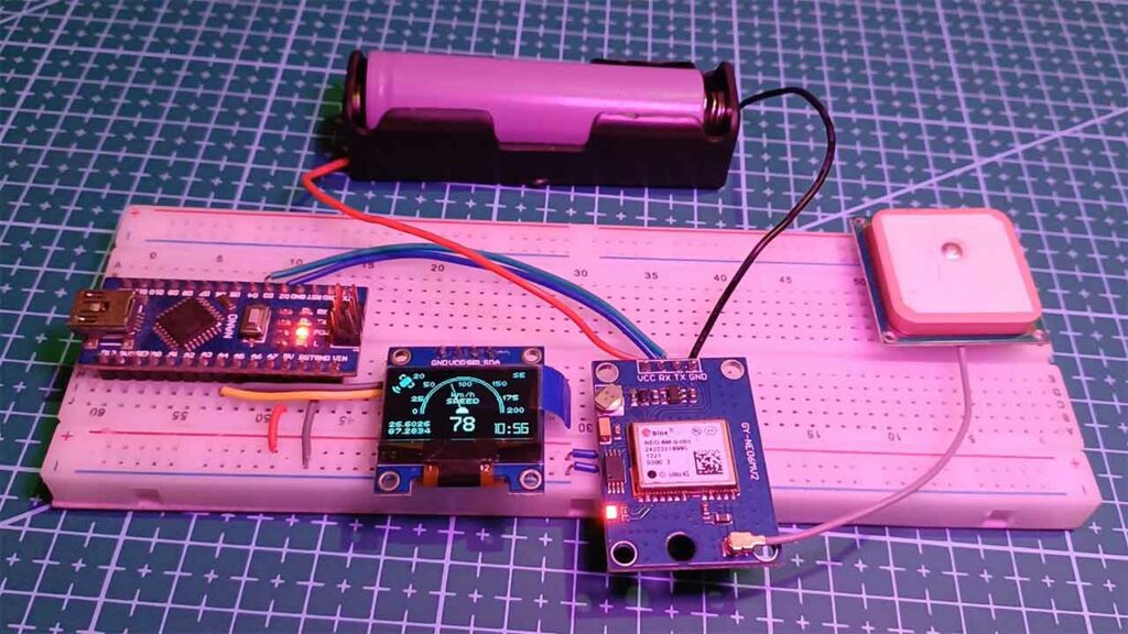
Arduino Speedometer on OLED Display
Once your GPS module receives the enough signal and connects with enough number of satellites, the OLED Display will display the speed in kilometers per hour (KPH) or in Miles per hour (MPH) in analog as well as on digital format.
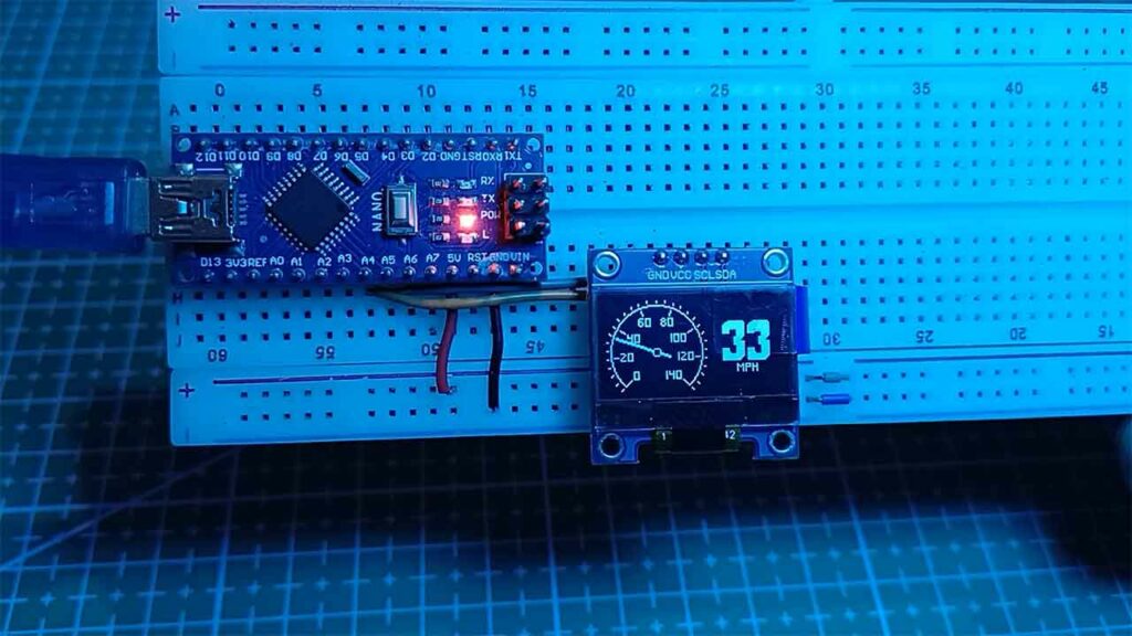
In a stationary condition or when the device is not in motion the speed displayed on the OLED Display is Zero. The accuracy of the speed readings can be influenced by factors such as signal strength, satellite visibility, and environmental conditions.