FPGA Basics: Components, Architecture, and Applications
Understanding FPGA Basics: Components, Architecture, and Applications
What is the FPGA?
FPGA, or field programmable gate array, is a type of Embedded IC that, like PLDs, may be configured to create virtually any system or digital circuit. PLDS can support only a few hundred gates, but FPGAs can accommodate thousands of gates. A language called HDL (Hardware Description Language), which is comparable to the language used for an ASIC (Application Specific Integrated Circuit), is typically used to specify the setting of the FPGA design.
When compared to ASIC technologies with fixed functions, like conventional cells, FPGAs can offer a variety of benefits. ASICs typically take months to create and cost thousands of dollars to purchase the device. However, FPGAs may be made in less than a second, and they can cost anything from a few dollars to a few thousand. The FPGA’s flexibility has a hefty price tag in terms of space, power, and delay. An FPGA uses 20 to 35 times more space than a conventional cell ASIC while performing at speeds that are 3 to 4 times slower. This article talks about the fundamentals of FPGAs and the switch matrix, logic blocks, and I/O pad of the FPGA architecture module.
FPGA Architecture
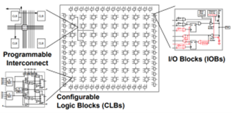
There are three different sorts of modules in the typical FPGA architecture. They are Configurable Logic Blocks (CLB), Switch Matrix/Interconnection Wires, and I/O blocks or Pads. The fundamental FPGA architecture consists of two-dimensional arrays of logic blocks that can be connected in any order by the user. The following is a discussion of an FPGA architecture module’s functions:
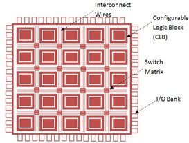
- Digital inputs, outputs, and logic are all included in a CLB (Configurable Logic Block). It carries out user logic.
- Interconnects give the logic blocks direction so they can implement the user logic.
- The switch matrix offers switching between interconnects according to the logic.
- I/O pads are utilized to connect many applications to the outside world.
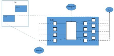
The MUX (Multiplexer), D flip-flop, and LUT components of a logic block. The MUX is utilized for selection logic, the LUT implements combinational logical functions, and a D flip flop stores the output of the LUT. The Look Up Table-based function generator is the fundamental component of the FPGA. Following tests, the LUT can have 3, 4, 6, or even 8 inputs. We now have adaptive LUTs, which use two function generators to implement two outputs from a single LUT.
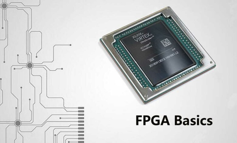
The most well-known FPGA, the Xilinx Virtex-5, has a flip-flop and a look-up table (LUT) that are coupled by MUX. Thousands or hundreds of customizable logic blocks make up the modern FPGA. Modelsim and Xilinx ISE software are used for development and to create a bitstream file for setting the FPGA.
Components of FPGA
Let’s now look more closely at how an FPGA is built. Typically, an FPGA comprises three basic components. as follows: Programmable Routing, Programmable IO Blocks, and Programmable Logic Cells (or Logic Blocks).
Logic Block
The logic block in Xilinx-based FPGAs is referred to as Configurable Logic Blocks (CLB), whereas equivalent structures in Altera-based FPGAs are known as Logic Array Blocks (LAB). In this conversation, let’s use the acronym CLB. A CLB is the core component of an FPGA with logic and storage capabilities. The fundamental logic block can be implemented using transistors, NAND gates, multiplexors, look-up tables (LUTs), PAL-like structures, or even CPUs. The logic and storage functionalities are implemented by Xilinx and Altera using Look-up Table (LUT) based logic blocks.
A basic logic element can be a single basic logic element or a group of connected basic logic elements. A basic logic element is a combination of a flip-flop and a look-up table (which is made up of SRAM and multiplexors).
The 2n configuration bits that make up a LUT with ‘n’ inputs are implemented using SRAM cells. These 2n SRAM Bits can be used by the LUT to implement any logical operation.
Programmable Routing
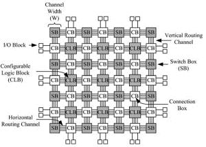
The programmable routing network is in charge of connecting the Logic Blocks if the Logic Blocks are responsible for supplying the computational capabilities. The routing network provides connections between each logic block and between the logic block and the IO Block, allowing for the complete creation of a custom circuit. The basic building blocks of the routing network are joined lines with programmable switches that can be configured in any computer language. In general, routing designs can be divided into two groups. They are island-style routing and hierarchical routing.
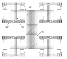
The two-dimensional array of logic blocks is arranged, and an island-style routing architecture is used to connect them. Such routing is frequently used in commercial FPGAs. Hierarchical routing design takes advantage of the fact that many logic blocks are limited to a small set of connections by organizing the logic blocks into various groups or clusters. In the event that the logic blocks are housed in the same cluster, hierarchical routing links them at a low level of hierarchy. Wiring is done at a higher level of the hierarchical structure when logic blocks are dispersed throughout several clusters.
IO Blocks
The programmable input and output unit known as the IOB (Input Output Block) serves as the link between external circuits and FPGA. used to meet the requirements for driving and synchronizing input/output signals under different electrical characteristics.
An FPGA’s IOB is divided into numerous banks for administration purposes and to enable adaptability to different electrical standards. The interface standard of each bank is determined by the VCCO interface voltage. There can be more than one VCCO for a single bank, but there can only be one VCCO per bank. Ports can only be joined if they correspond to the same electrical standard. The equal VCCO voltage is a fundamental criterion of the interface standard.
FPGA Applications
FPGAs are helpful for a variety of applications, which has led to their explosive rise over the past ten years. Digital signal processing, bioinformatics, device controllers, software-defined radio, random logic, ASIC prototyping, medical imaging, computer hardware emulation, integrating multiple SPLDs, voice recognition, cryptography, filtering, communication encoding, and many other applications are examples of applications where an FPGA is specifically used.
FPGAs are typically reserved for niche vertical applications with low manufacturing volumes. The top firms spend in hardware costs per unit for these low-volume applications. The range of feasible applications has now been expanded by enhanced performance dynamics and cost.
ASIC prototyping, audio, automotive, broadcast, consumer electronics, distributed monetary systems, data centers, high-performance computing, industrial, medical, scientific instruments, security systems, video & image processing, wired communications, and wireless communications are some of the more popular FPGA applications.
Types of FPGAs Based on Applications
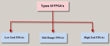
According to their intended use, Field Programmable Gate Arrays are divided into three categories: Low-end, mid-range, and high-end FPGAs.
Low-End FPGAs
These FPGAs are made with low power requirements, low logic densities, and low chip complexity in mind. Examples of low-end FPGAs include the Mach XO/ICE40 from Lattice Semiconductor, the Spartan family from Xilinx, the Cyclone family from Altera, and the Fusion family from Microsemi.
Mid-Range FPGAs
These FPGAs were created as a compromise between performance and price and are the best option between low-end and high-end FPGAs. Examples of mid-range FPGAs include the Altera Arria, Xlinix Artix-7/Kintex-7 series, Microsemi IGL002, and Lattice Semiconductor’s ECP3 and ECP5 series.
High-End FPGAs
These FPGAs are designed for maximum performance and logic density. The Stratix family from Altera, the Virtex family from Xilinx, the Speedster 22i family from Achronix, and the ProASIC3 family from Microsemi are examples of high-end FPGAs.

